Kaynes Semiconductor Packaging Explained – What Role do they play in Semi-conductor ecosystem?
When people think about the semiconductor industry, they usually focus on chip design or fabrication plants. However, before a semiconductor chip can power a smartphone, vehicle, or industrial machine, it must go through an equally important stage- packaging and testing.
This is where Kaynes Technology is making its entry into the semiconductor value chain. Through its OSAT facility, the company aims to participate in one of the fastest-growing segments of the semiconductor ecosystem.
What is Semiconductor Packaging?
Semiconductor packaging is the process of enclosing a manufactured chip in a protective package that allows it to connect with electronic devices and function reliably in real-world conditions.
Without packaging, semiconductor chips would be too fragile to handle and integrate into products. Packaging also helps improve performance, heat management, and electrical connectivity.
Where Does Packaging Fit in the Semiconductor Value Chain?
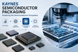
The semiconductor ecosystem consists of multiple stages, including chip design, wafer fabrication, packaging, testing, and final integration into electronic products.
Packaging sits between chip manufacturing and end-use applications. Once chips are fabricated, they are assembled, packaged, and tested before being shipped to device manufacturers. This makes packaging a critical link in the overall semiconductor supply chain.
Why is Advanced Packaging Becoming More Important?
Advanced packaging is becoming increasingly important because semiconductor scaling is slowing. Instead of relying solely on smaller transistor nodes, companies are increasingly using chiplets and multi-chip architectures. Industry leaders such as NVIDIA, AMD and Intel are investing heavily in advanced packaging technologies to improve computing performance without proportionately increasing manufacturing complexity.
According to industry estimates, the global semiconductor packaging market is expected to grow from approximately $35-40 billion today to over $60 billion by 2030, driven by AI accelerators, high-performance computing, automotive electronics, and advanced chip architectures.
Kaynes’ Entry into Semiconductor Packaging
Kaynes has entered the semiconductor packaging space through its OSAT (Outsourced Semiconductor Assembly and Test) business. This allows the company to move beyond traditional electronics manufacturing and participate in a higher-value segment of the electronics ecosystem.
The company is enhancing its backward integration with a planned capex of about Rs. 3,300 Cr for OSAT to be completed in phases over the next 3–5 years.
A notable milestone was the company’s successful shipment of India’s first commercially manufactured Multi-Chip Module from its OSAT facility, highlighting its growing capabilities in advanced semiconductor packaging. This has been explained in detail in our Kaynes Technology stock analysis video.
Why This Matters for Kaynes
Semiconductor packaging offers better value addition compared to conventional electronics manufacturing. It also creates opportunities to serve industries such as automotive, industrial electronics, defense, and telecommunications.
As India develops its semiconductor ecosystem, companies with packaging and testing capabilities could benefit from rising domestic demand and government support for semiconductor localization.
Kaynes’ OSAT Growth Plans
Kaynes’ semiconductor packaging ambitions are gradually moving from development to commercialization. While Unit 1 is already operational, Unit 2 is expected to enter commercialization in Q2 FY26, helping expand the company’s OSAT capabilities.
Management has indicated revenue visibility of over ₹2,500 crore over the next five years. Interestingly, the business is expected to be export-focused initially, targeting global customers rather than the domestic market.
What Should Investors Watch?
For FY27, management expects OSAT revenues of around ₹250–300 crore as commercialization ramps up. While still in the early stages, this provides a glimpse into the business’s long-term potential.
If execution remains on track and customer adoption increases, semiconductor packaging could emerge as an important growth driver for Kaynes in the coming years.
Opportunities and Challenges
The growth opportunity is significant as global demand for semiconductor packaging continues to increase. India’s push toward semiconductor self-reliance and electronics manufacturing could further accelerate adoption.
The OSAT business typically requires high utilization levels to achieve attractive profitability. Delays in customer onboarding, lower-than-expected capacity utilization, or technology obsolescence could impact returns on invested capital.
Conclusion
Semiconductor packaging may not attract as much attention as chip fabrication, but it is an essential part of the semiconductor ecosystem. Without packaging and testing, semiconductor chips cannot be used in real-world applications.
For Kaynes Technology, its entry into OSAT and advanced packaging represents an opportunity to move higher up the value chain. If executed successfully, semiconductor packaging could become an important growth driver in the company’s long-term strategy.
Check Other Post Posts
-
 Waaree Energies: Tariffs, Order Book & Future Outlook
March 25, 2026
-
What is IMPS in Bank?
November 23, 2024